Lauterbach Teardowns
Written 2024-02-27
Tags:Lauterbach Debugging
I was curious what was inside the Lauterbach debug tips (also called probe heads around here). For the unfamiliar, the Lauterbach power-debug system consists of two parts. The first part is a universal module that connects to a PC over USB or Ethernet, or in the old days parallel. The second part adapts the debug-cable port on the module to a specific JTAG or SWD target, like 20-pin ARM. I took apart two of mine.
LA-7742(ARM9)
I like this one because while Lauterbach generally sticks to a Vintage 1990s hardware design, this LA-7742 seems even older. If you look closely, the housing says W. Germany.


This one consists of a 24C02 serial flash and a ALVC164245 level translating tri-state buffer.


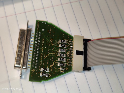
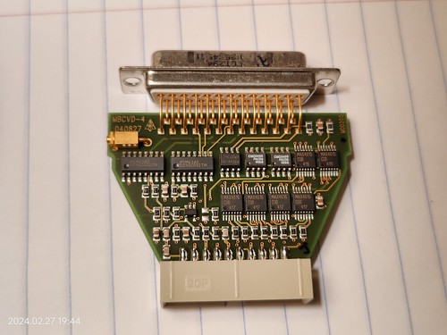
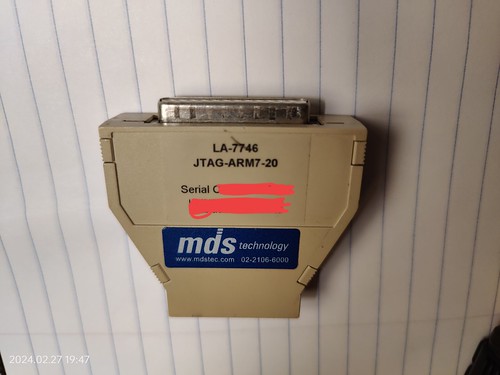
LA-7747(ARM7)
This one looks like the current debug adapter cables, except with a 20pin IDC socket rather than pigtail. even though it is for an older core design than the LA-7742.

Inside it appears more complicated, and seems be the same 24C02 serial flash, but instead has MAX4615/6 analog switches, DS90C032 quad differential receivers, and some PACDN006 ESD diode packs.